Competence Hub: Uppsala

Anchored by Sweden’s largest academic cleanroom, Uppsala strengthens Sweden’s chip agenda through materials, device prototyping and test access - especially for life-science instrumentation, sensors and energy-related electronics.

The Uppsala innovation ecosystem

  • Uppsala University – Sweden’s oldest university and a globally recognized research institution advancing materials science, semiconductor electronics, nanotechnology, quantum physics, renewable energy systems, and next-generation biomaterials.

  • Ångström Laboratory – One of Europe’s leading research facilities for physics, materials science, chemistry, and engineering, providing advanced infrastructure for semiconductor research, prototyping, and technology development.

  • Myfab Uppsala – Sweden’s largest academic cleanroom facility for micro- and nanofabrication, offering open-access labs for semiconductor processing, thin-film deposition, materials characterization, and device prototyping.

  • STUNS – A regional collaboration platform connecting academia, industry, and the public sector to strengthen innovation across sectors including energy, life science, and advanced materials.

  • Uppsala Science Park – A major innovation hub hosting technology, life science, and engineering companies, providing close access to university expertise, specialized infrastructure, and collaborative research environments.

  • Uppsala Business Park – A commercial innovation cluster focused on life science and advanced technology, offering laboratories, business services, and a strong regional network for growing companies.

  • Uppsala Innovation Centre (UIC) – One of Sweden’s leading startup incubators, supporting early-stage companies with business development, funding advisory, and scaling strategies for deeptech and science-based ventures.

  • Innovation Hub Uppsala – Strengthens the regional innovation pipeline by supporting early-stage entrepreneurs through advisory services, networks, and ecosystem coordination across emerging technology fields.

  • ALMI – A national financing and advisory organization providing loans, venture capital, and business development support to help small and medium-sized companies grow and scale.

From materials to prototypes: Uppsala’s role in Sweden’s semiconductor ecosystem

The Uppsala region is one of Sweden’s most dynamic and rapidly expanding knowledge hubs, driven by strong research environments, leading innovation ecosystems, and a diverse business community ranging from global industrial companies to small, entrepreneur‑led firms. With its strategic location near Arlanda Airport and strong connections to Stockholm, Uppsala has developed into a central node with two internationally leading universities, a top‑tier innovation support system, and a labour market that attracts highly skilled talent.

The region is particularly research‑intensive and plays a strategic role in Sweden’s semiconductor ecosystem: home to Sweden’s largest academic cleanroom facility and deep expertise in materials science, nanotechnology, and energy-related technologies. Uppsala also hosts a broad industrial base that relies on advanced semiconductor‑enabled components in sensor systems, instrumentation, and energy applications such as solar power and battery technology. This makes the region essential for early innovation, prototyping, materials development, and training the next generation of specialists. Uppsala’s strengths are further reinforced by its internationally recognised life science cluster. Here, universities, companies, and public actors collaborate closely on research, development, and industrial applications.

Myfab Uppsala and the Uppsala innovation system

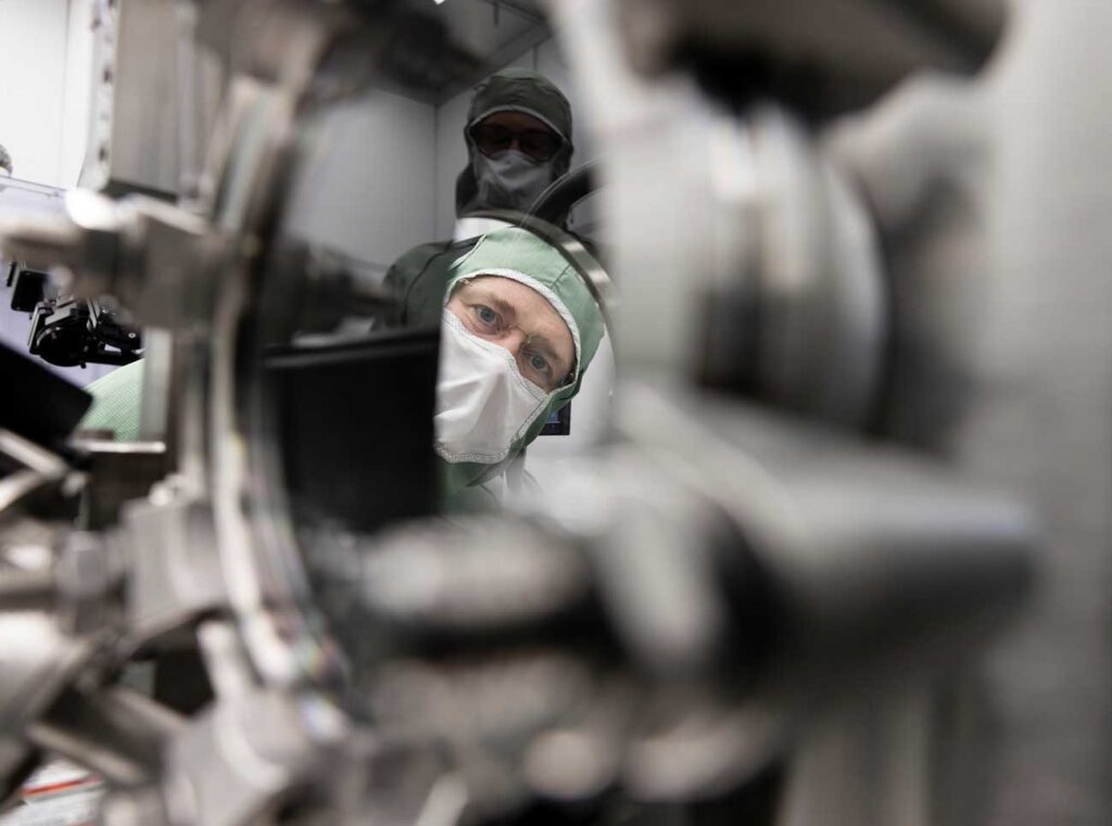
Uppsala University is a globally recognized institution with leading expertise in materials science, nanotechnology, solid‑state physics, micro‑ and nanofabrication, quantum‑adjacent technologies, and energy‑related semiconductor materials. The university hosts the Ångström Laboratory, where Myfab Uppsala, Sweden’s largest academic cleanroom, is a node in the national research infrastructure for micro‑ and nanofabrication. Myfab Uppsala provides open‑access facilities for advanced R&D, materials characterisation, device processing, lithography, thin‑film engineering and prototyping used by both researchers and companies.

Picture from the cleanroom facilities in Ångströms Laboratory.

The innovation ecosystem is mature and well‑structured. Organisations such as STUNS, Uppsala Science Park, Uppsala Business Park, and university innovation offices work together to support commercialisation, business development and cluster growth. Uppsala Innovation Centre (UIC) and the broader Innovation Hub Uppsala provide strong support structures for deeptech startups and SMEs working with semiconductor‑relevant technologies, including sensors, instrumentation, materials and energy systems.

The region’s Smart Specialisation Strategy 2022–2027 further strengthens this foundation by focusing on challenge‑driven and knowledge‑intensive innovation in areas where Uppsala has distinctive advantages — life science, sustainability, energy, advanced technology, and complex societal challenges.

Future growth and collaboration: semiconductor’s Uppsala

Myfab Uppsala recently received substantial national and EU Chips Act–linked investment to expand semiconductor‑relevant capability explicitly aimed at strengthening Sweden’s semiconductor R&D capacity. In Uppsala, upgrades explicitly include student involvement in semiconductor cleanroom activity, ensuring early exposure and strengthened recruitment pipelines. The investments make Uppsala essential for Sweden’s positioning in semiconductor materials R&D, nano‑ and microfabrication prototyping, instrumentation and sensor development, energy and electrification technologies and deeptech life‑science instrumentation, and places Uppsala as a core national R&D node, enabling prototyping, early‑stage device development, and process innovation used by companies and researchers across Sweden.

Innovative semiconductor-related companies in the Uppsala region

For updates or to highlight additional actors in this regional high-level overview, please contact us

Sensors and microwaves

  • Comheat Microwave – Develops high-performance electronic components and subsystems for microwave and RF applications used in research, industry, and advanced technology systems.

  • Percy Roc AB – Provides AI-driven technologies and customized solutions for industrial heating processes, helping manufacturers optimize performance, efficiency, and control.

  • ScandiNova – A world-leading provider of solid-state, high-power pulse modulators and RF units used in scientific research, medical technology, and advanced industrial applications.

  • SweSenSi – Develops advanced sensor technologies and measurement systems for industrial monitoring and precision sensing in demanding environments.

Solar energy

  • First Solar European Technology Center – The Swedish R&D center of global solar company First Solar, focusing on innovation in high-efficiency thin-film photovoltaic technologies.

  • Midsummer – Develops lightweight and flexible thin-film solar panels and production equipment designed for distributed energy generation and building-integrated photovoltaics.

Space

  • AAC Clyde Space – Develops small satellite technologies and data services that enable applications such as environmental monitoring, weather forecasting, and precision agriculture.

  • APR Technologies – A deep-tech company delivering advanced thermal management and electronics cooling solutions for aerospace, ICT infrastructure, and electrification systems.

Life science & medtech

  • Probingon AB – Develops clinical-grade wearable diagnostics and IoMT technologies that enable continuous health monitoring and improved data-driven healthcare.

  • ScandiDos – Develops advanced quality assurance systems for radiotherapy, helping clinics deliver safer and more precise cancer treatments.

Others

  • Acuvi – PiezoMotor – Develops precision micro-motion technologies based on piezoelectric materials used in diagnostics, semiconductor manufacturing, and optical instrumentation.

  • Chromogenics – Develops electrochromic smart glass that dynamically controls light and heat in buildings to improve energy efficiency and indoor comfort.

Share this post:

Related blog posts

Check out the latest from us

Open source silicon and why access matter

Interview with Olof Kindgren, Senior Digital Design Engineer at Qamcom and co-founder of the FOSSi...

Read more

From semiconductors to systems

Interview with Jan Grahn, professor at Chalmers University of Technology, on high-frequency semiconductor technology for...

Read more

Competence hub: Kista-Stockholm

As Sweden’s semiconductor landscape expands, Kista-Stockholm stands out as one of its key hubs. Anchored...

Read more